- 您现在的位置:买卖IC网 > Sheet目录1996 > HMC704LP4E (Hittite Microwave Corporation)IC FRACT-N PLL 16BIT 24QFN
P
LL
s
-
s
M
T
5 - 33
HMC704LP4E
v03.1211
8 GHz fractionaL-n PLL
For price, delivery, and to place orders: Hittite Microwave Corporation,20 Alpha Road, Chelmsford, MA 01824
Phone: 978-250-3343
Fax: 978-250-3373
Order On-line at www.hittite.com
Application Support: Phone: 978-250-3343 or apps@hittite.com
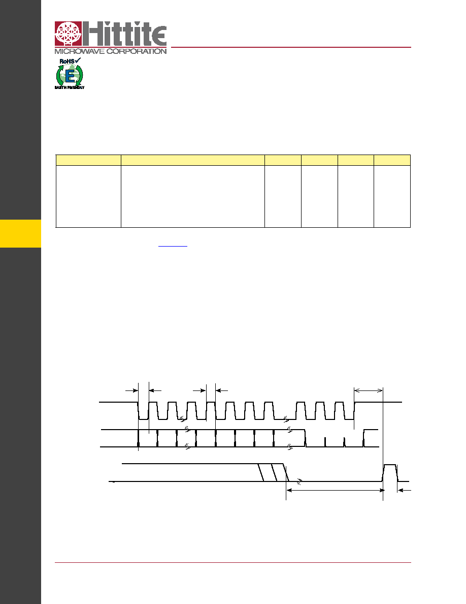
open Mode - Serial Port WritE operation
AVDD = DVDD = 3.3V +/-10%, AGND = DGND = 0V
table 11. SPi open Mode - Write timing characteristics
Parameter
Conditions
Min.
Typ.
Max.
Units
t1
t2
t3
t4
t5
sDI setup time
sDI hold time
sEN low duration
sEN high duration
sCLK 32 Rising Edge to sEN Rising Edge
serial port Clock speed
3
1
10
DC
50
ns
MHz
A typical WRITE cycle is shown in Figure 38.
a. The Master (host) places 24 bit data, d23:d0, MsB first, on sDI on the first 24 falling edges of sCLK.
b. the slave (PLL) shifts in data on sDI on the first 24 rising edges of sCLK
c. Master places 5 bit register address to be written to, r4:r0, MsB first, on the next 5 falling edges of
sCLK (25-29)
d. slave shifts the register bits on the next 5 rising edges of sCLK (25-29).
e. Master places 3 bit chip address, a2:a0, MsB first, on the next 3 falling edges of sCLK (30-32).
Hittite reserves chip address a2:a0 = 000 for all RF PLL-VCOs.
f.
slave shifts the chip address bits on the next 3 rising edges of sCLK (30-32).
g. Master asserts sEN after the 32nd rising edge of sCLK.
h. slave registers the sDI data on the rising edge of sEN.
i.
Master clears sEN to complete the WRITE cycle.
t1
Figure 38. Open Mode - Serial Port Timing Diagram - WRITE
sCLK
sDI
d22
d2
d1
d0
r4
r3
a2
a1
a0
x
r0
2
3
22
23
24
25
26
31
32
x
t2
sEN
t4
t5
t3
发布紧急采购,3分钟左右您将得到回复。
相关PDF资料
HMC830LP6GE
IC FRACT-N PLL W/VCO 40QFN
HMP8117CNZ
IC VIDEO DECODER NTSC/PAL 80PQFP
HMP8156ACNZ
IC VIDEO ENCODER NTSC/PAL 64MQFP
HSP45102SC-40Z
IC OSC NCO 40MHZ 28-SOIC
HSP45106JC-33Z
IC OSC NCO 33MHZ 84-PLCC
HSP45116AVC-52Z
IC OSC NCO 52MHZ 160-MQFP
ICL7109EPL+
IC ADC 12BIT 3-ST 40-DIP
ICM7217AIPI
IC OSC UP/DWN CNTR 2MHZ 28-DIP
相关代理商/技术参数
HMC704LP4ETR
制造商:Hittite Microwave Corp 功能描述:IC FRACT-N PLL 16BIT 24QFN
HMC705LP4
制造商:HITTITE 制造商全称:Hittite Microwave Corporation 功能描述:6.5 GHz PROGRAMMABLE DIVIDER (N = 1 - 17)
HMC705LP4E
制造商:Hittite Microwave Corp 功能描述:IC DIVIDER HBT PROGR 24-QFN
HMC705LP4ETR
功能描述:IC DIVIDER HBT PROGR 24QFN 制造商:analog devices inc. 系列:- 包装:剪切带(CT) 零件状态:在售 功能:分频器 频率:100MHz ~ 6.5GHz RF 类型:- 辅助属性:- 封装/外壳:24-VFQFN 裸露焊盘 供应商器件封装:24-QFN(4x4) 标准包装:1
hmc706lc3c
制造商:Hittite Microwave Corp 功能描述:IC CONV NRZ-RZ 13GBPS 16SMD
HMC707LP5
制造商:HITTITE 制造商全称:Hittite Microwave Corporation 功能描述:0.5 dB LSB 6-BIT DIGITAL VARIABLE GAIN AMPLIFIER, 700 - 1200 MHz
HMC707LP5_10
制造商:HITTITE 制造商全称:Hittite Microwave Corporation 功能描述:0.5 dB LSB 6-BIT DIGITAL VARIABLE GAIN AMPLIFIER, 700 - 1200 MHz
HMC707LP5E
制造商:Hittite Microwave Corp 功能描述:IC AMP DVGA LNA 6-BIT 32-QFN